The III-V Lab celebrates 20 years of creating semiconductors
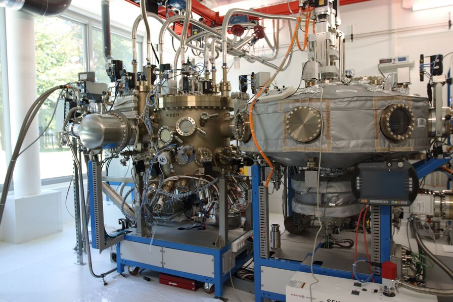
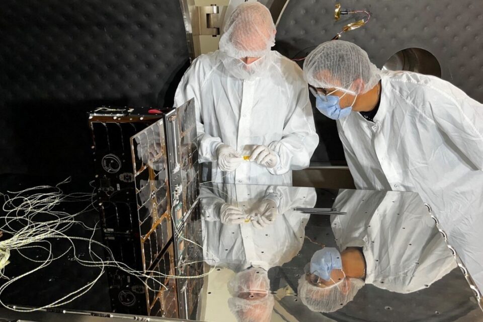
Focused on the integration of III and V materials onto silicon wafers, the III-V Lab was founded in 2004 by Nokia and Thales and later joined by CEA in 2011. Now based in Paris-Saclay, the lab uses a machine occupying almost the entire width of one of its clean rooms to apply successive layers of III-V material onto silicon wafers, endowing them with special properties for a wide range of applications in nanotechnologies, photonics, microelectronics and other markets. Situated within a bustling scientific environment, the lab fosters collaboration between universities, institutes, industrial groups and startups working with semiconductors.